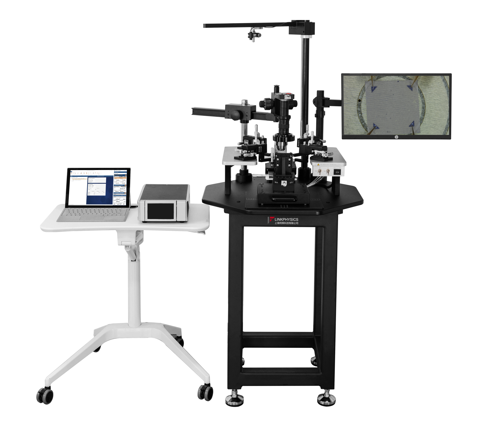
The HSPM-05PS Room Temperature Probe Hall Test System provides a vertical magnetic field environment for 8-inch samples and devices to be tested. External connection of other electrical test instruments allows non-destructive electrical testing of chips, wafers and devices at room temperature, such as current, voltage, resistance and other electrical signals under different magnetic fields.
Features:
-Stable dual displacement adjustment system that adjusts the displacement of the sample holder and probe arm.
-The sample holder can hold 8-inch wafer samples, with porous zoned controlled gas adsorption fixation.
-Automatic control of the permanent magnet's forward and backward motion and N.S. pole flip, and can be accurately positioned, the magnetic field size of 0.5T.
-6 probe arms can be installed.
-The probe arms are adsorbed by magnets, which can be moved arbitrarily and can be adjusted in three dimensions for easy operation and precise pinning, and the probes of the four probe arms can be pinned to any position of the samples.
-The probe arm adopts three coaxial cables and three coaxial connectors, the leakage current is small, within 100fA.
-CCD magnification is 180 times, working distance is 100mm.
Test materials:
- Thermoelectric materials: bismuth telluride, lead telluride, silicon-germanium alloys, etc.
- Photovoltaic materials/solar cells: (A silicon (monocrystalline silicon, amorphous silicon), CIGS (copper indium gallium selenide), cadmium telluride, chalcogenide, etc.)
- Organic Materials: (OFET, OLED)
- Transparent Conductive Metal Oxide TCO: (ITO, AZO, ZnO, IGZO (Indium Gallium Zinc Oxide), etc.)
- Semiconductor materials: SiGe, InAs, SiC, InGaAs, GaN, SiC, InP, ZnO, Ga2O3, etc.
- Two-dimensional materials: graphene, BN, MoS2, etc.