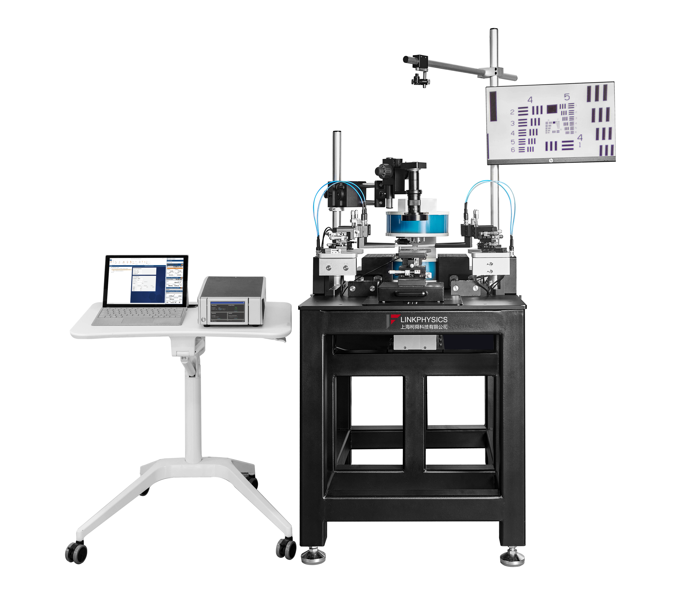
The HSEM-06PS Room Temperature Variable Field Probe Bench Hall Test System provides a vertically variable magnetic field environment for 4-inch samples and devices to be tested. External connections to other electrical test instruments allow non-destructive electrical testing of chips, wafers and devices at room temperature, such as electrical signals such as current, voltage, resistance, etc. under different magnetic fields.
Features:
- Sample holder holds 4" wafer samples with porous zoned controlled gas adsorption fixation. (Other sizes can be customised)
- Capable of providing variable magnetic field environments with magnetic field sizes ±0.6T
- 6 probe arms can be mounted
- The probe arms are magnetised and can be moved at will, and can be fine-tuned in three dimensions for easy operation and accurate pinning, and the probes of the four arms can be pinned to any position of the sample.
- The probe arm adopts tri-coaxial cable and tri-coaxial connector, the leakage current is small, within 100fA.
- CCD magnification is 180 times, working distance is 100mm.
Test materials:
- Thermoelectric materials: bismuth telluride, lead telluride, silicon-germanium alloys, etc.
- Photovoltaic materials/solar cells: (A silicon (monocrystalline silicon, amorphous silicon), CIGS (copper indium gallium selenide), cadmium telluride, chalcogenide, etc.)
- Organic Materials: (OFET, OLED)
- Transparent Conductive Metal Oxide TCO: (ITO, AZO, ZnO, IGZO (Indium Gallium Zinc Oxide), etc.)
- Semiconductor materials: SiGe, InAs, SiC, InGaAs, GaN, SiC, InP, ZnO, Ga2O3, etc.
- Two-dimensional materials: graphene, BN, MoS2, etc.